Strategies to Enable Assured Access to Semiconductors for the Department of Defense (2024)
Chapter: 2 The Competitive Position of the United States in the Semiconductor Sector
2
The Competitive Position of the United States in the Semiconductor Sector
The committee was asked to review the competitive position of the United States in the global semiconductor ecosystem, including a review of the industrial policies in other nations in semiconductor and related critical technologies. This chapter discusses the history of the United States in the global semiconductor ecosystem as well as the current state of the U.S. semiconductor sector compared with other nations. There is a focus throughout on the Department of Defense’s (DoD’s) semiconductor needs and its potential role in strengthening the semiconductor sector broadly.
THE POSITION OF THE U.S. SEMICONDUCTOR SECTOR
The current U.S. competitive position in semiconductors has been the recent subject of many thorough studies,1 so this section will not attempt to duplicate those reports and will instead draw from them. This discussion summarizes the
___________________
1Those reports include the following: W. Hunt, 2022, “Sustaining U.S. Competitiveness in Semiconductor Manufacturing,” Center for Security and Emerging Technology (CSET), Georgetown University, January, https://cset.georgetown.edu/publication/sustaining-u-s-competitiveness-in-semiconductor-manufacturing; M. Griffith and S. Goguichvili, 2021, “The U.S. Needs a Sustained, Comprehensive and Cohesive Semiconductor National Security Effort,” Woodrow Wilson Center, https://www.wilsoncenter.org/blog-post/us-needs-sustained-comprehensive-and-cohesive-semiconductor-national-security-effort; C. Miller, 2022, Chip War, The Fight for the World’s Most Critical Technology, New York: Simon and Schuster; S. Kahn, A. Mann, and D. Peterson, 2021, “The Semiconductor Supply Chain: Assessing National Competitiveness, Center for Security and Emerging Technology,” January, https://cset.georgetown.edu/publication/the-semiconductor-supply-chain; President’s Council of Advisors on Science and Technology (PCAST), 2022, Report to the President on Revitalizing the Semiconductor Ecosystem, White House, September, https://www.whitehouse.gov/wp-content/uploads/2022/09/PCAST_Semiconductors-Report_Sep2022.pdf; Defense Science Board, 2022, Ensuring Microelectronics Superiority, https://dsb.cto.mil/wp-content/uploads/dsb/site/wwwroot/reports/2020s/Microelectronics_ExSumm.pdf; R. Palma, T. Sexton, R. Varadarajan, T. Baker, and A. Bhatia, 2022, “How the US Can Strengthen the Global Semiconductor Ecosystem.” Boston Consulting Group,” https://www.bcg.com/publications/2022/how-the-us-can-strengthen-the-global-semiconductor-industry; Semiconductor Industry Association (SIA), 2023, State of the U.S. Semiconductor Industry, https://www.semiconductors.org/wp-content/uploads/2023/07/SIA_State-of-Industry-Report_2023_Final_072723.pdf; SIA, 2021, State of the U.S. Semiconductor Industry, https://www.semiconductors.org/wp-content/uploads/2021/09/2021-SIA-State-of-the-Industry-Report.pdf; A. Varas, R. Varadarajian, J. Goodrich, and F. Yinug, 2020, “Turning the Tide for Semiconductor Manufacturing in the US,” SIA and Boston Consulting Group, https://www.semiconductors.org/wp-content/uploads/2020/09/Government-Incentives-and-US-Competitiveness-in-Semiconductor-Manufacturing-Sep-2020.pdf; SIA and Oxford Economics, 2023, Chipping Away, Assessing and Addressing the Labor Market Gap Facing the U.S. Semiconductor Industry, July, https://www.semiconductors.org/wp-content/uploads/2023/07/SIA_July2023_ChippingAway_website.pdf; SIA and Boston Consulting Group, 2021, Strengthening the Global Semiconductor Supply Chain in an Uncertain Era, https://www.semiconductors.org/wp-content/uploads/2021/05/BCG-x-SIA-Strengthening-the-Global-Semiconductor-Value-Chain-April-2021_1.pdf; Institute for Defense Analysis, 2016, Semiconductor Industrial Base Focus Study–Final Report, IDA D-8294, December, https://www.ida.org/-/media/feature/publications/s/se/semiconductor-industrial-base-focus-study—final-report/d-8294.ashx; PCAST, 2017, Report to the President: Ensuring Long-Term U.S. Leadership in Semiconductors, January, https://obamawhitehouse.archives.gov/sites/default/files/microsites/ostp/PCAST/pcast_ensuring_long-term_us_leadership_in_semiconductors.pdf; Office of Science and Technology Policy (OSTP), 2022, “Draft National Strategy for Microelectronics Research,” https://www.whitehouse.gov/wp-content/uploads/2022/09/SML-DRAFT-Microlectronics-Strategy-For-Public-Comment.pdf; Department of Commerce (DOC), 2023, Assessment of the Status of the Microelectronics Industrial Base in the United States, Bureau of Industry and Security, Office of Technology Evaluation, December, https://www.bis.doc.gov/index.php/documents/technology-evaluation/3402-section-9904-report-final-20231221/file.
historical role of the federal government in public–private partnerships (PPPs) with the semiconductor sector, the importance of semiconductors as an enabling technology for national security and the overall economy, and the current state of the U.S. semiconductor sector. It discusses the strengths and weaknesses of the overall industrial ecosystem for semiconductors in the United States and the national security implications of semiconductor production in the United States, given current geopolitical considerations. Industrial policies and investments in other nations are noted as well as recent U.S. government actions. Barriers to a resilient domestic semiconductor sector are enumerated with corresponding findings, with a particular focus on DoD’s role and needs. Potential elements that could be considered for a DoD semiconductor strategy, including a PPP mechanism, are considered at the end, with recommendations for steps to increase resilience.
This report comes at a similar time as the 2023 release of DoD’s first National Defense Industrial Strategy.2 That document noted that “the events of recent years dramatically exposed serious shortfalls in both domestic manufacturing and international supply chains … [demonstrating] America’s near wholesale dependency on other nations for many products and materials crucial to modern life.” It found that “China became the global industrial powerhouse in many key areas—from shipbuilding to critical minerals to microelectronics… . [It] exceeds the capacity of not just the United States, but the combined output of our key European and Asian allies as well.”3 It concluded:
We need to shift from policies rooted in the 20th century that supported a narrow defense industrial base, capitalized on the DoD as the monopsony power, and promoted either/or tradeoffs between cost, speed, and scale. We need to build a modernized industrial ecosystem that includes the traditional defense contractors—the [Defense Industrial Base] primes and sub-tier defense contractors who provide equipment and services—and also includes innovative new technology developers; academia; research laboratories; technical centers; manufacturing centers of excellence; service providers; government-owned, contractor-operated facilities; and finance streams, especially private equity and venture capital.4
This proposed approach highlights broader economic security as an essential foundation for traditional national security. It encompasses a growing concern about microelectronics supply resilience and the growing importance of the semiconductor industry. Accordingly, DoD is currently taking a broader look at the overall capability and capacity of the U.S. semiconductor sector. Of course, this is not the first time DoD has been actively involved in the microelectronics sector.
___________________
2Department of Defense (DoD), 2023, National Defense Industrial Strategy, https://www.businessdefense.gov/docs/ndis/2023-NDIS.pdf, p. 8.
3Ibid.
4DoD. 2023. National Defense Industrial Strategy, p. 9.
PRIOR PERIODS OF GOVERNMENT-SUPPORTED SEMICONDUCTOR PUBLIC–PRIVATE PARTNERSHIPS
Semiconductor electronic components5 have been recognized for at least six decades as a foundational technology for implementation of computer, communications, and information technology systems. Chips are now embedded in virtually every device—they have become as essential to information processing as oil was to energy consumption in the second half of the 20th century, or steel to the first half, only more so. They are essential for defense technologies and systems.6 By annual global sales, semiconductors are now a U.S. $500 billion industry, and are on a path to become a trillion-dollar industry by 2030.7 Leading-edge semiconductors are essential for a range of advanced technologies today, as well as for near-future disruptive technologies, particularly artificial intelligence (AI), machine learning (ML), and quantum information systems (QISs),8 but also for autonomous vehicles and clean energy solutions—all of which have significant national security dimensions. And, of course, they are the core infrastructure hardware component required for a host of societal services, such as the Internet and broadband wireless services, upon which the daily functioning of societies is now based. To sustain the current rate of technology advances, semiconductor sector companies spend more on research and development (R&D) than almost any other sector, reinvesting about one-fifth of revenue annually. U.S.-headquartered companies alone reported spending $60.2 billion on R&D in 2023.9
Defining Public–Private Partnerships
The U.S. government is currently launching its third large-scale PPP intervention in this sector. The committee notes that there is no standard, internationally
___________________
5In this context, components include a wide array of devices used in electronic systems, ranging from passive devices, such as transistors and capacitors, to active devices, such as logic chips.
6DoD, for example, has contracted with Intel for secure semiconductor foundry services as part of its Rapid Assured Microelectronics Prototypes-Commercial (RAMP-C) program to build up domestic design and production of cutting-edge semiconductor chips. Other firms are also involved in the consortium. D. Sebastian, 2021, “Intel Wins Defense Department Award for Domestic Chip Making,” Wall Street Journal, August 23, https://www.wsj.com/articles/intel-wins-defense-department-award-for-domestic-chip-making-11629726220.
7O. Burkacky, J. Dragon, and N. Lehman, 2022, “The Semiconductor Decade: A Trillion Dollar Industry,” https://www.mckinsey.com/industries/semiconductors/our-insights/the-semiconductor-decade-a-trillion-dollar-industry.
8See, for example, S.W. Huang, S. Han, W. Lee, et al., 2020, “Symbiosis of Semiconductors, AI and Quantum Computing,” IEEE International Electron Devices Meeting (IEDM), 19.1.1–19.1.6, https://ieeexplore.ieee.org/document/9372061.
9SIA, 2024, “Industry Factsheet,” https://www.semiconductors.org/wp-content/uploads/2024/04/SIA-Industry-Factsheet-2024.pdf.
accepted definition of PPPs. Different nations and agencies have adopted different working definitions. Typically, PPPs involve agreements to provide a public asset or service in which both public and private parties have risks and responsibilities.10 By sharing risks and capabilities across the sector to achieve a public mission, they can enable outcomes that the public sector alone cannot achieve.11 Objectives for PPP agreements include such goals as establishing a clear and predictable framework for public and private parties, with specific resource commitments; grounding the agreement in value for money; and using budget transparency to limit risks and ensure the integrity of the agreement.12 DoD has long utilized PPPs and has even issued guidelines for creating PPPs for product support. This document broadly defines PPPs as contractual collaborations between DoD and nonfederal parties where both parties leverage the expertise, resources, and incentives of the other to achieve mutually agreed-on goals.13 Mutual benefits are a hallmark, and a broad range of activities beyond product support fit within this framework, from information sharing to R&D to joint development projects. Chapter 4 further elaborates on DoD’s use of PPPs.
The First Period: Department of Defense Support for Integrated Circuits
The first DoD semiconductor PPP effort was in the 1950s and 1960s, when military and space users worked with industry to insert advanced, cutting-edge semiconductors into defense and space systems in order to achieve qualitative military superiority for the United States during the Cold War conflict with the former Soviet Union.14 A rich menu of subsidies for R&D, manufacturing technology
___________________
10World Bank, “About PPPLRC and PPPs,” https://ppp.worldbank.org/public-private-partnership/about-us/about-public-private-partnerships, accessed July 30, 2024.
11International Monetary Fund, 2001, “Public Private Partnerships,” Finance and Development 38(3), https://www.imf.org/external/pubs/ft/fandd/2001/09/gerrard.htm.
12OECD, 2012, “Principles for Public Governance of Public-Private Partnerships,” https://www.oecd.org/governance/budgeting/PPP-Recommendation.pdf.
13DoD, 2016, Public-Private Partnering for Product Support Guidebook, https://www.acq.osd.mil/log/mr/.policy.html/PPP_for_Product_Support_Guidebook_Oct2016.pdf.
14See A. Slomovic, 1988, “Anteing Up: The Government’s Role in the Microelectronics Industry,” RAND Corporation, https://apps.dtic.mil/sti/pdfs/ADA228267.pdf. Almost 50 percent of semiconductor R&D was paid for by government users over this period (K. Flamm, 1996, “Mismanaged Trade? Strategic Policy in the Semiconductor Industry,” Washington: Brookings Institution, p. 36). The federal government’s share of the market for discrete semiconductors (individual transistors and diodes) peaked at about 50 percent in 1960 (Flamm, 1996, p. 34; Slomovic, 1988, p. 21; N.J. Asher and L.J. Strom, 1977, “The Role of the Department Defense in the Development of Integrated Circuits,” Arlington, VA: Institute for Defense Analysis, https://apps.dtic.mil/sti/tr/pdf/ADA048610.pdf, p. 10). Military and space applications initially accounted for the entirety of the integrated circuit (IC) market when commercial sales of these leading-edge semiconductors commenced in the early 1960s and accounted for the majority of sales through the late 1960s (Flamm, 1996, p. 34; Asher and Strom, 1977, p. 26; Slomovic, 1988, p. 29).
refinement, and new capacity investment was devised, as defense and space systems designers stepped forward and worked with early commercial semiconductor suppliers to provide the initial market for what were initially very costly new electronic components.15 At this time, DoD played a critical market support role. Integrated circuits were first invented in 1959 and first shipped in 1961. DoD and NASA were almost the only customers for the first 4 years of production.16 Costs and prices dropped quickly and dramatically, however, stimulated by a rapidly expanding commercial demand for semiconductors in a variety of new applications. As the size of the military market relative to the commercial market declined through the 1970s, military demand started to become less relevant to leading-edge technological innovation in semiconductors, and the close partnerships between DoD and industry faded.
The Second Period: Support for SEMATECH
The second major PPP intervention in the semiconductor sector began in the mid-1980s. Although transistors, integrated circuits, and a host of semiconductor advances were initially developed in the United States, by the mid-1980s, the U.S. semiconductor manufacturing industry was falling behind that of Japan. For one critical process technology, photolithography, the Japanese firms Nikon and Canon had developed technologies that surpassed that of U.S. equipment manufacturers. Japan’s semiconductor firms had been working together closely with the relevant materials and equipment manufacturers under the aegis of a collaborative industrial R&D consortia funded by its Ministry of International Trade and Industry (MITI) to achieve this goal. That is, Japan utilized a PPP to gain a leadership position in lithography equipment and processes. Japanese manufacturers also had access to lower-cost financing for investments in leading-edge capacity. By the 1970s and early 1980s, Japan’s investments in new manufacturing capacity exceeded that of the United States, and it was clear that the United States was losing its leadership position.17
In response, a group of U.S. semiconductor CEOs persuaded the Reagan administration to fund a PPP to restore U.S. semiconductor manufacturing technology
___________________
15Asher and Strom, 1977.
16DoD and NASA bought 100 percent of integrated circuit production in 1961 and 1962, 85 percent in 1963 and 1964, and 72 percent in 1965 (see C. Fishman, 2019, “How NASA Gave Birth to Modern Computing,” Fast Company, June 13, https://www.fastcompany.com/90362753/how-nasa-gave-birth-to-modern-computing-and-gets-no-credit-for-it).
17See K. Flamm, 1996, “Mismanaged Trade: Strategic Policy and the Semiconductor Industry,” Washington, DC: Brooking Institution Press, c. 10. More generally, on the political economy of this Japanese public–private partnership, see C. Johnson, 1982, MITI and the Japanese Miracle—The Growth of Industrial Policy, 1925–1975, Palo Alto, CA: Stanford University Press.
leadership. A public–private consortium, Semiconductor Manufacturing Technology (SEMATECH), was founded in 1987 with 14 leading semiconductor companies.18 In a reflection of the importance of this new PPP, the first chief executive of SEMATECH to be appointed was Robert Noyce, co-founder of Intel. The Defense Advanced Research Projects Agency (DARPA) administered the government’s investment, amounting to $500 million over 5 years, which was matched by the industry participants.19
SEMATECH’s initial targets were to demonstrate production semiconductor chips with a critical dimension of 0.8 micrometers by 1989, 0.5 micrometers by 1990, and 0.35 micrometers by 1992, all using American-made equipment.20 By the mid-1990s, these objectives were achieved, and a turnaround in U.S. producers’ market share was evident, as shown in Figure 2-1. (Note, however, that this figure displays sales by company headquarters location, not manufacturing location.) At that time, a thoroughly globalized materials and equipment industry was in place, Japan’s ascendancy had plateaued, and the U.S. chip industry was seemingly again on sound footing; hence, the SEMATECH restriction to using only American-made equipment for manufacturing seemed increasingly impractical and irrelevant.21
In July 1994, the SEMATECH board of directors adopted a resolution thanking the federal government for its partnership, which had successfully spurred industry’s turnaround and helped the United States regain world competitiveness. Anticipating the domestic industry’s continued good health, the SEMATECH board of directors voted to transfer all of SEMATECH’s operations to private funding beginning in 1997. With the end of public sector matching funds, this effectively brought the formal industry–government PPP for SEMATECH to an end. However, SEMATECH sought continuing participation by DARPA and DoD as observers on its board of directors and technical advisory boards, and DoD and
___________________
18L. Berlin, 2005, The Man Behind the Microchip: Robert Noyce and the Invention of Silicon Valley, Oxford, UK: Oxford University Press, pp. 257–305; R. Hof, 2011, “Lessons from SEMATECH,” MIT Technology Review, July 25, https://www.technologyreview.com/2011/07/25/192832/lessons-from-sematech.
19L.D. Browning and J. Shetler, 2000, “SEMATECH: Saving the U.S. Semiconductor Industry,” College Station, TX; Texas A&M Press. DARPA received additional funding after SEMATECH’s initial 5-year time horizon of 1987–1992, until 1994, for semiconductor R&D at SEMATECH as well as at universities and other entities (General Accounting Office, Federal Research, 1992, “SEMATECH’s Technological Progress and Proposed R&D Program,” GAO/RCED-92-223BR, July, https://www.gao.gov/assets/rced-92-223br.pdf; General Accounting Office, 1992, “Federal Research, Lessons Learned from SEMATECH,” GAO/RCED-92-283, September 11, https://www.gao.gov/assets/rced-92-283.pdf).
20J.B. Horrigan, 1999, “Cooperating Competitors: A Comparison of MCC and SEMATECH,” Monograph, National Research Council.
21Semiconductor Technology Council, 1996, First Annual Report, September, https://www.esd.whs.mil/Portals/54/Documents/FOID/Reading%20Room/DARPA/10-F-0709_Semiconductor_Technology_Council_First_Annual_Report_September1996.pdf, pp. 3–13.
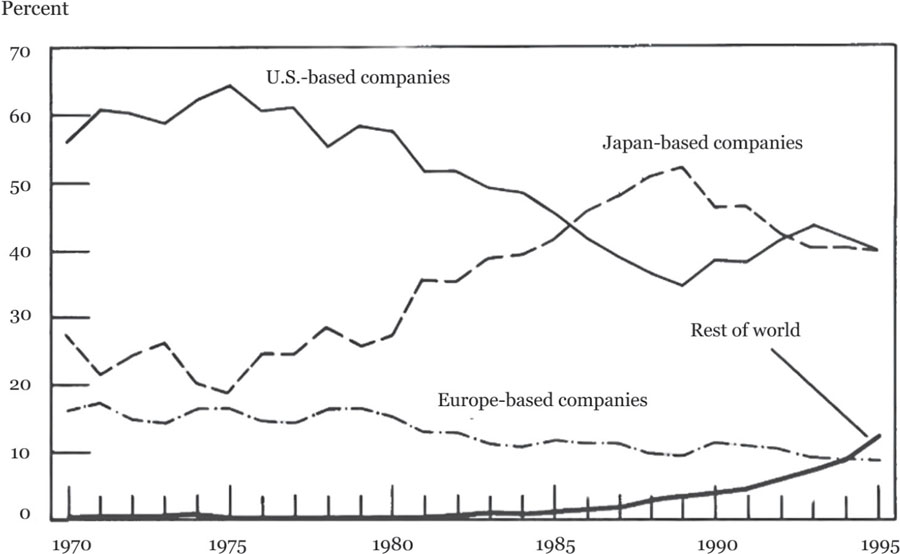
SOURCE: K. Flamm, 1996, Mismanaged Trade: Strategic Policy and the Semiconductor Industry, Washington, DC: Brookings Institution Press.
DARPA remained active participants in many ongoing SEMATECH technology-related activities.22
___________________
22In its final report to DoD, SEMATECH wrote that “SEMATECH and DoD should continue cooperation beyond 1997. There is no requirement that the existing cooperative framework (e.g., the grant agreement, memorandum of understanding, and enabling legislation) be terminated. Elements of the framework for continued cooperation include but are not limited to DARPA should continue its participation as a non-voting observer on the SEMATECH board of directors and the Executive Technical Advisory Board. DARPA (or a DoD designee of their choice) is encouraged to attend meetings of the focus technical advisory boards and project technical advisory boards. DARPA and SEMATECH should conduct a joint annual review, during which the annual operating and long-range strategic plans of each organization will be shared. (DARPA should share no government classified information with SEMATECH during the course of such reviews.) SEMATECH should continue to be an invited participant in meetings of the Semiconductor Technology Council. Because SEMATECH has ceased to seek federal funds, the possibility of formal SEMATECH representation on the STC should be considered… . SEMATECH will continue the use of all assets purchased with regular (commingled) operating funds, unless and until dissolution of the corporation.”
Equally notable was SEMATECH’s list of elements not to be part of the ongoing cooperation framework: “SEMATECH will no longer be subject to audits by the GAO or other federal audit or oversight agencies… . SEMATECH will no longer be subject to the regulations and requirements set forth in OMB circulars A-110, A-122 and A-133.” (SEMATECH, 1997, SEMATECH 1987–1997, A Final Report to the Department of Defense, February 21, https://www.esd.whs.mil/Portals/54/Documents/FOID/Reading%20Room/Science_and_Technology/10-F-0709_A_Final_Report_to_the_Department_of_Defense_February_21_1987.pdf, pp. 12–13).
This decision reflected three realities of that moment.23 First, renewing federal funding for SEMATECH would have required a new legislative initiative, and the U.S. semiconductor industry was not ready to invest the necessary political capital, given the apparent success already achieved in reestablishing U.S. industry’s competitive position. Second, leading-edge semiconductor manufacturing technology was being transformed into a globalized infrastructure, with best-in-class equipment and materials available from friendly foreign sources. The U.S. semiconductor industry leaders supported the globalization tide,24 and the prevalent view at DoD was that by incorporating global technology leaders into SEMATECH, including suppliers based in allied nations, the U.S. military would be able to ensure U.S. industrial and defense access to the very best available semiconductor technology. The globalization of SEMATECH might also have been seen as problematic from the standpoint of seeking new legislation to provide federal support to SEMATECH. Third, at that time, “about 60 percent of SEMATECH’s annual budget was being expended on external R&D efforts,”25 and both SEMATECH and DoD leadership viewed the National Science Foundation (NSF), DARPA, and the nonprofit Semiconductor Research Corporation as having better capabilities to identify and fund long-range R&D on next-generation semiconductor manufacturing innovation.
In response to these developments, SEMATECH underwent two structural changes in the mid-1990s. First, it became a truly international consortium, reflecting the continuing globalization of the semiconductor manufacturing, equipment, and materials ecosystem. In 1996, “SEMATECH established the International 300 mm Initiative (I300I), a subsidiary organization with international membership … a major technology and infrastructure development initiative to lead its membership and their equipment suppliers in the conversion to 300 mm diameter wafers.”26 A few years later, SEMATECH would change its name to International SEMATECH and invite foreign members to join—and join they did.27
___________________
23This description is based on the recollections of Kenneth Flamm, who was serving as DoD’s top dual-use technology policy official at the time and was charged with interfacing with SEMATECH’s CEO and top leadership, and of William B. Bonvillian, who was serving as a senior advisor in the U.S. Senate working on these issues at that time.
24The U.S. semiconductor industry had been one of the very first U.S. industries to move the bulk of its most labor-intensive operations (chip assembly and packaging) offshore in the mid-1960s. See K. Flamm, 1985, “Internationalization in the Semiconductor Industry,” in J. Grunwald and K. Flamm, The Global Factory, Washington, DC: Brookings Institution.
25Semiconductor Technology Council, 1996, First Annual Report, pp. 3–13.
26Semiconductor Technology Council, 1996, First Annual Report, pp. 4–5.
27By 2006, full international members of SEMATECH included Philips, Infineon, and Samsung. In addition to these firms, TSMC, Panasonic/Matsushita Electric, Spansion, NEC, and Renesas were members of the I300I subsidiary.
Second, SEMATECH shifted its focus to developing semiconductor manufacturing standards and coordinating the technological improvements needed to ensure successful and timely introduction of new semiconductor manufacturing technology “nodes” using products from the many suppliers making up the global semiconductor industrial base. SEMATECH had been “organized into thrust areas that are aligned with the Semiconductor Industry Association’s (SIA’s) National Technology Roadmap for Semiconductors.”27 The development and commercialization of the next generation of lithography tools and processes (at a wavelength of 193 nm), and the coordinated development of new tools able to use larger-diameter wafers (at 300 mm) were the first R&D thrust areas chosen by SEMATECH following these changes.28
SEMATECH’s (and the U.S. semiconductor industry’s) embrace of industry globalization also included pivoting its stewardship of the National Technology Roadmap for Semiconductors effort to instead developing an International Technology Roadmap for Semiconductors (ITRS), and using that as the vehicle to coordinate and accelerate semiconductor manufacturing technology development on a global scale.28 SEMATECH became the administrative hub for the ITRS and provided a unique and useful service to a global semiconductor industry in coordinating the development and deployment of new technology nodes through the first half decade of the 21st century.
These new institutional arrangements seemed to work well for SEMATECH through the beginning of the new millennium, but then seemed to flounder. Arguably, the fundamental problem was economics. With rapidly increasing economies of scale at each new generation of manufacturing technology, fewer and fewer firms were willing or able to invest in building expensive semiconductor wafer fabrication plants, known as fabs, that used cutting-edge semiconductor technology. Indeed, leading-edge semiconductor manufacturing was becoming an increasingly concentrated industry. SEMATECH evolved into a technology coordination entity in which only a few of its members were likely to invest in the next generation of manufacturing technology. Having a large group of bystander firms making decisions about technology priorities that would affect a much smaller group of firms that were likely to make the needed investments became an untenable organizational structure. With the industry’s recovery, DoD and the federal government in following years had only a limited engagement with the industry and were not prepared to consider future subsidies to offset those deployed by other nations to capture market share. In 2003, SEMATECH entered into a partnership
___________________
27By 2006, full international members of SEMATECH included Philips, Infineon, and Samsung. In addition to these firms, TSMC, Panasonic/Matsushita Electric, Spansion, NEC, and Renesas were members of the I300I subsidiary.
28For a more detailed discussion of the ITRS, see K. Flamm, 2009, “Economic Impacts of International R&D Coordination: SEMATECH and the International Technology Roadmap,” pp. 108–125 in National Research Council, 2009, 21st Century Innovation Systems for Japan and the United States: Lessons from a Decade of Change: Report of a Symposium. Washington, DC: The National Academies Press. https://doi.org/10.17226/12194.
with the State of New York’s SUNY Polytechnic in Albany, subsequently relocating to Albany, and in 2010 folded its operations into SUNY Poly with some leading members withdrawing, effectively ending the program.29
Defense Advanced Research Projects Agency Support for Semiconductor Advances
Keys to the success of SEMATECH as a PPP during its early years included the following: bringing in top technical talent from industry partners for 1- or 2-year assignments; the personal commitment of industry CEOs; leadership that encouraged innovative thinking; a no-nonsense attitude toward dropping noncompetitive approaches; collaborative development of roadmaps for future industry-wide technology goals; and DARPA’s close cooperation, which encouraged close coordination among the private partners.30
DoD also made a series of smaller-scale semiconductor research investments with industry and academic researchers in the years before and after SEMATECH. Perhaps most notable was work in the late 1970s by researchers at the California Institute of Technology (Caltech) and Xerox Palo Alto Research Center (PARC) to develop a greatly improved system for Very Large Scale Integration (VLSI) chip design using advanced software tools.31 Development of these tools was a key enabler for the separation of chip design from chip manufacturing, and the development
___________________
29R. Van Steenburg, 2022, “With the CHIPS Down, Sematech Gets Second Look,” National Defense, June 2, https://www.nationaldefensemagazine.org/articles/2022/6/2/with-chips-down-sematech-gets-second-look; C. Wessner and T. Howell, 2023, “Implementing the CHIPS Act: SEMATECH’s Lessons for the National Semiconductor Technology Center,” CSIS, May 19, https://www.csis.org/analysis/implementing-chips-act-sematechs-lessons-national-semiconductor-technology-center; M. Lapels, 2015, “Semiconductor R&D Crisis?” Semiconductor Engineering, June 11, https://semiengineering.com/semiconductor-rd-crisis.
30See, for example, P. Grindley, D. Mowery, and B. Silverman, 1994, “SEMATECH and Collaborative Research: Lessons in the Design of High-Technology Consortia,” Journal of Policy Analysis and Management, https://www.academia.edu/15457838; G. Moore, 2003, “The SEMATECH Contribution,” pp. 96–104 in National Research Council, 2003, Securing the Future: Regional and National Programs to Support the Semiconductor Industry. Washington, DC: The National Academies Press, https://doi.org/10.17226/10677; General Accounting Office, 1992, Lessons Learned from SEMATECH, GAO/RECD 92-283, September, https://www.gao.gov/assets/rced-92-283.pdf; A.N. Link, D.J. Teece, and W. Finan, 1996, “Estimating the Benefits from Collaboration: The Case of SEMATECH,” Review of Industrial Organization 11(5):737–751, https://www.jstor.org/stable/41798663; K. Flamm, 2009, “Economic Impacts of International R&D Coordination: SEMATECH and the International Technology Roadmap,” in National Research Council, 2009, 21st Century Innovation Systems for Japan and the United States: Lessons from a Decade of Change: Report of a Symposium, Washington, DC: The National Academies Press, https://doi.org/10.17226/12194.
31See T.S. Perry and P. Wallich, 1985, “Xerox Parc’s Engineers on How They Invented the Future,” IEEE Spectrum, October 1, https://spectrum.ieee.org/xerox-parc.
of fabless (design-only, without fabrication plants) and foundry (manufacturing-only) chip firms followed. This work had been supported by around $100 million in government funding by 1982, via direct investments rather than through a PPP structure.32
Xerox PARC’s efforts in the late 1970s to offer a fast-turnaround VLSI prototyping service allowed researchers to submit chip designs as digital files uploaded remotely to cooperating chip manufacturers for the first time. This system became the basis for a DARPA-supported chip prototyping service known as Metal Oxide Semiconductor Implementation Service (MOSIS), which continues to serve university and industry researchers, hosted by the University of Southern California.33
Requests from different researchers were pooled into common lots and run through the fabrication process, after which completed chips were returned to the researchers. This system obviated the need for direct access to a fabrication line or for dealing with the complexity of arranging fabrication time at an industrial facility, by providing access to a qualified group of fabrication facilities through a single interface. Prominent VLSI researcher Charles Seitz commented that MOSIS represented the first period since the pioneering work of Eckert and Mauchley on the ENIAC in the late 1940s that universities and small companies had access to state-of-the-art digital technology.34
This service effort (which grew from 258 projects in 1981 to 1,880 in 1989)35 may have provided some of the inspiration, as well as some of the early software infrastructure,36 for the pure-play foundry business model developed by Taiwan Semiconductor Manufacturing Company (TSMC) when it was founded by Morris Chang in Taiwan in 1987.37
___________________
32See Chapter 4, “The Organization of Federal Support: A Historical Review,” in National Research Council, 1999, Funding a Revolution: Government Support for Computing Research, Washington, DC: National Academy Press. https://doi.org/10.17226/6323.
33The MOSIS Service. See https://www.themosisservice.com.
34National Research Council, 1999, Funding a Revolution, p. 121.
35Ibid.
36“At the time, the interface between the foundry and the design group was fairly simple. The foundry would produce design rules and SPICE parameters for the designers; the design would be given back to the foundry as a GDSII file and a test program. Basic standard cells were required, and these were available on the open market from companies like Artisan, or some groups would design their own.” See D. Nenni, 2023, “The TSMC OIP Backstory,” SemiWiki [blog], September 18, https://semiwiki.com/semiconductor-manufacturers/tsmc/335155-the-tsmc-oip-backstory; on DARPA funding of SPICE and other chip design tools, see K. Flamm, 1987, Targeting the Computer, Washington, DC: Brookings Institution, p. 69.
37For a more complete description of these efforts, see Chapter 4, “The Organization of Federal Support: A Historical Review,” in National Research Council, 1999, Funding a Revolution.
DARPA also funded advances in semiconductor lithography and in computing, from personal computing to computer graphics.38 The Very High-Speed Integrated Circuit (VHSIC) program was an R&D effort from 1979–1988 through a DoD–industry partnership featuring joint government–industry planning, large-scale industry participation, and multi-firm collaboration to speed improvements and adoption of submicron integrated circuits. In contrast to the later SEMATECH effort, VHSIC’s objective was to incorporate cutting-edge semiconductor technology in defense-unique chips, and then into new systems built by DoD’s largest contractors, to thus widen the technological advantage relative to the former Soviet Union. Because the scale of production of chips going into weapons systems was so much smaller than the rapidly expanding commercial marketplace, and because security restrictions hindered incorporation of the technology developed into commercial products, the initiative was terminated in 1990, with the commercial sector having moved ahead of DoD’s technologies. Nonetheless, the VHSIC program made some important technological contributions to the semiconductor industry. In particular, in parallel with DARPA’s VLSI program, VHSIC funded the development of electronic design automation (EDA) tools and a hardware description language, VHSIC Hardware Description Language (VHDL), which ultimately evolved into the chip design software tools in use today.39 While falling short of SEMATECH in both scale and outcome, VHSIC was a notable response to a well-publicized effort in Japan by MITI (the VLSI Project), with five major Japanese electronics firms targeting commercial IC markets that proved to be very successful.40
DARPA’s investments in advanced lithography were similarly closely coordinated with industry. Over a 14-year period from fiscal year (FY) 1991 to FY 2005, DARPA’s advanced lithography program distributed an estimated $1 billion to firms exploring next-generation lithography (NGL) approaches.41 DARPA supported the semiconductor industry’s exploration of electron beam lithography, ion projection lithography, and X-ray proximity lithography, as well as extreme ultraviolet (EUV) lithography. EUV ultimately emerged as the preferred NGL technology, with Intel,
___________________
38See, for example, M.M. Waldrop, 2001, Dream Machine: J.C.R. Licklider and the Revolution That Made Computing Personal, New York: Penguin Books, p. 201.
39See R. Reitmeyer, 1981, “CAD for Military Systems, an Essential Link to LSI, VLSI and VHSIC Technology,” IEEE DAC, Design Automation Conference, https://ieeexplore.ieee.org/xpl/conhome/10567/proceeding.
40G.R. Fong, 1986, “The Potential for Industrial Policy, Lessons from the Very High Speed Integrated Circuit Program,” Journal of Policy Analysis and Management 5(2), https://www.academia.edu/5757279/The_potential_for_industrial_policy_Lessons_from_the_very_high_speed_integrated_circuit_program.
41EE Times, 2005, “DARPA Ends Litho Aid at Critical Juncture for Maskless,” https://www.eetimes.com/darpa-ends-litho-aid-at-critical-juncture-for-maskless.
AMD, and Motorola funding a PPP for EUV development with three Department of Energy laboratories.42
These are only some of the examples of smaller-scale federal semiconductor investments in PPPs that were successful. But by 2020, the United States again faced a loss in chip technology leadership.
CURRENT STATE OF THE U.S. SEMICONDUCTOR SECTOR AS COMPARED WITH OTHER NATIONS
Today’s concerns about the decline in U.S. semiconductor leadership arise against the backdrop of the ever-increasing importance of semiconductors to industrialization, economic development, and global prosperity. Other nations have increased R&D investments in the semiconductor sector, and the motivations for these investments are easily understood. More than 50 percent of the global supply of semiconductor chips produced annually is consumed by China today, as it is the largest assembler of consumer electronics.43 That is, China’s prosperity is dependent on sustained access to semiconductor supply, including from U.S. companies, many of which have higher sales in China than in the United States,44 and China is committed to strengthening and supporting its semiconductor sector across the entire value chain. As has been noted elsewhere, while the United States once clearly led in total science R&D, China is expected to pass the United States in overall governmental R&D investment across all fields in coming years.45 Asian nations are pursuing carefully defined technology strategies that include R&D and support of applications and production, while the United States historically has avoided such strategies, except for the defense sector, and episodically, in agriculture, transportation and communications, pharmaceuticals and biotechnology, and aerospace.
Although the United States has offshored much of its electronics production, in 2022 semiconductors were still its largest electronic product export and its
___________________
42Intel, 1997, “Government-Industry Partnership to Develop Advanced Lithography Technology,” News Release, September 11, https://www.intel.com/pressroom/archive/releases/1997/CN091197. HTM; Intel, 2001, “Partners Unveil First Extreme Ultraviolet Chip-Making Machine,” News Release, April 11, https://www.intel.com/pressroom/archive/releases/2001/20010411tech.htm.
43D. Araya, 2024, “Will China Dominate the Global Semiconductor Market?” Center for International Governance Innovation, https://www.cigionline.org/articles/will-china-dominate-the-global-semiconductor-market.
44D. Butts and S. Chiang, 2024, “China Remains Crucial for U.S. Chipmakers Amid Rising Tensions Between the World’s Top Two Economies,” CNBC, April 12, https://www.cnbc.com/2024/04/12/china-remains-a-crucial-market-for-us-chipmakers-amid-rising-tensions-.html.
45National Science Board, Science and Engineering Indicators, 2020, U.S. Trends and International Comparisons, NSBV 20-3, https://eric.ed.gov/?id=ED615506.
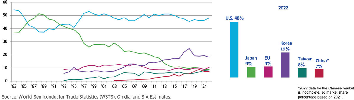
SOURCE: Courtesy of Semiconductor Industry Association (SIA).
fifth-largest export product, amounting to approximately $61 billion. Companies based in the United States—including both fabless design houses and integrated device manufacturers (IDMs) and their foreign production subsidiaries—held 48 percent of the global semiconductor market in 2022.46 Figure 2-2 shows that after reversing its decline in global market share in the early 1990s (depicted in Figure 2-1), U.S.-based semiconductor companies continued to capture a stable share (roughly half) of global chip sales from 1996 until today. Semiconductor fabs are located in some 18 U.S. states and employ some 345,000 people.47
Despite those impressive-sounding numbers, only 12 percent of the world’s semiconductors (by value of sales) were fabricated in the United States in 2022, compared with 37 percent in 1990.48 Much of the capacity of leading U.S.-headquartered chipmakers is now located offshore. Intel, for example, has 61 percent of its manufacturing capacity offshore, and Micron, the Unites States’ only producer of memory chips, has 79 percent of its production capacity overseas.49
___________________
46Semiconductor Industry Association (SIA), 2023, 2023 State of the U.S. Semiconductor Industry, https://www.semiconductors.org/wp-content/uploads/2023/08/SIA_State-of-Industry-Report_2023_Final_080323.pdf.
47SIA, 2023, 2023 State of the U.S. Semiconductor Industry, pp. 9–10; SIA and Oxford Economics, 2021, Chipping in: The U.S. Semiconductor Industry Workforce and How Federal Incentives Will Increase Domestic Jobs, SIA, May, https://www.semiconductors.org/wp-content/uploads/2021/05/SIA-Impact_May2021-FINAL-May-19-2021_2.pdf, pp. 11–15.
48A. Varas, R. Varadarajian, J. Goodrich, and F. Yinug, 2020, “Turning the Tide for Semiconductor Manufacturing in the US,” SIA and Boston Consulting Group, September 6, semiconductors.org/wp-content/uploads/2020/09/Government-Incentives-and-US-Competitiveness-in-Semiconductor-Manufacturing-Sep-2020.pdf.
49Hunt, 2022, “Sustaining U.S. Competitiveness in Semiconductor Manufacturing.”
Eighty percent of semiconductor sales by U.S. companies are in overseas markets.50 And most significantly, by 2018, firms in Taiwan and South Korea (i.e., TSMC and Samsung) had taken technology leadership in producing the most advanced semiconductors (at the 5 nm node).51
Leadership in Semiconductor Manufacturing by Nations
The estimated share of global production and related efforts carried out in the United States in different semiconductor subsectors, according to a recent Department of Commerce (DOC) study,52 is as follows:
- R&D: 47 percent
- Design: 27 percent
- Front-end (i.e., wafer-level) fabrication: 12 percent
- Assembly, testing, and packaging: <2 percent, with an additional estimate that 85 percent of chips sold by U.S.-based companies are packaged in Taiwan, China, South Korea, or Malaysia
None of the world’s current most advanced chips (at the 5 nm node) were produced in the United States in 2023.
China has invested heavily in semiconductors, starting in the early 2000s.53 While it does not today have technology leadership, it now has a major presence in older node chip production, and is expected to grow to produce up to 40 percent of world chip supply by 2030.54 Its government investments specifically in
___________________
50SIA, 2020, “Comments of the SIA on Advanced Notice Regarding the Identification and Review of Controls for Certain Foundational Technologies,” November 9, https://www.semiconductors.org/wp-content/uploads/2020/11/SIA-Foundational-Comments-11-9-20.pdf.
51The term 5 nanometers (nm) does not refer to actual physical features such as gate length or to transistors being 5 nm in size. Rather, 5 nm is a term used in commercial practice by chipmakers to refer to an improved level of semiconductor chips that reflect a higher degree of miniaturization, increased speed, and reduced power consumption compared to the previous level of 7 nm.
52DOC, 2023, Assessment of the Status of the Microelectronics Industrial Base in the United States, Bureau of Industry and Security, Office of Technology Evaluation, December, https://www.bis.doc. gov/index.php/documents/technology-evaluation/3402-section-9904-report-final-20231221/file.
53See, for example, D. Ernst, 2014, “From Catching Up to Forging Ahead? China’s Prospects in Semiconductors,” East West Center Working Papers, 1, November, https://www.eastwestcenter.org/publications/catching-forging-ahead-chinas-prospects-in-semiconductors; D. Ernst, 2016, “China’s Bold Strategy for Semiconductors,” East West Center Working Paper, 9, September 1, https://www.eastwestcenter.org/publications/chinas-bold-strategy-semiconductors-zero-sum-game-or-catalyst-cooperation.
54A. Varas, R. Varadarajian, J. Goodrich, and F. Yinug, 2020, “Turning the Tide for Semiconductor Manufacturing in the US,” SIA and Boston Consulting Group, September 6, semiconductors.org/wp-content/uploads/2020/09/Government-Incentives-and-US-Competitiveness-in-Semiconductor-Manufacturing-Sep-2020.pdf, p. 10.
semiconductor research and technology development currently dwarf those of the U.S. government.55 Semiconductors are at the top of China’s list of sectors it hopes to dominate in the future—it has already systematically captured major markets in solar, wind, and battery technologies.56 As China’s chip production has ramped up in recent years, there is global concern that it will flood the world market to drive competitors out of the market, then dominate legacy chipmaking (meaning chips with critical dimensions larger than 14 nm), as it has done in other sectors.57
The world has become largely dependent on one semiconductor contract manufacturer, Taiwan’s TSMC, for producing chip designs that use the most advanced technology available.58 Today, TSMC produces the majority of the world’s high-end logic chips,59 which are found in virtually all electronic products, from computers to iPhones, and embedded in systems within automobiles and aircraft. With the world’s largest fabs, TSMC is the contract manufacturer for many well-known U.S. companies that design their own chips, such as Nvidia and Apple.60,61 TSMC was formed in 1987 by Morris Chang, a veteran of Texas Instruments, with significant backing from Taiwan’s government. TSMC created the dedicated integrated circuit foundry business model, only manufacturing chips for other firms based on those firms’ designs. This business model was made possible in part because of the VLSI design systems pioneered for DARPA. TSMC has now
___________________
55P. Triolo, 2021, “The Future of China’s Semiconductor Industry,” American Affairs 5(1), https://americanaffairsjournal.org/2021/02/the-future-of-chinas-semiconductor-industry; S. Ezell, 2021, “Moore’s Law Under Attack: The Impact of China’s Policies on Global Semiconductor Innovation,” Information Technology and Innovation Foundation, February 18, https://itif.org/publications/2021/02/18/moores-law-under-attack-impact-chinas-policies-global-semiconductor.
56X. Cen, V. Fos, and W. Jiang, 2022, “Race to Lead: How China’s Government Interventions Shape US-China Industrial Competition,” Stanford Center on China’s Economy and Institutions (paper), August 1, https://sccei.fsi.stanford.edu/china-briefs/race-lead-how-chinas-government-interventions-shape-us-china-industrial-competition.
57C. Miller, 2024, “Western Nations Need a Plan for When China Floods the Chip Market,” Financial Times, January 28, https://www.ft.com/content/2bd1c1a3-931a-4e95-9ea2-e1e8c635ff50.
58Y. Jie, S. Yang, and A. Fitch, 2021, “The World Relies on One Chip Maker in Taiwan,” Wall Street Journal, June 19, https://www.wsj.com/articles/the-world-relies-on-one-chip-maker-in-taiwan-leaving-everyone-vulnerable-11624075400.
59Miller, Chip War, 197, from Georgetown CSET and Semiconductor Industry Association data.
60K. Leswing, 2020, “Apple Is Breaking a 15-Year Partnership with Intel on Its Macs,” CNBC, November 10, https://www.cnbc.com/2020/11/10/why-apple-is-breaking-a-15-year-partnership-with-intel-on-its-macs-.html.
61Intel, which long emphasized production of chips of its own design, moved in 2021 toward a foundry approach, announcing plans for new foundries in Arizona at a cost of $20 billion (S. Nellis, 2021, “Intel to Spend $20 Billion on U.S. Chip Plants as CEO Challenges Asia Dominance,” Reuters, March 23, https://www.reuters.com/world/asia-pacific/intel-doubles-down-chip-manufacturing-plans-20-billion-new-arizona-sites-2021-03-23).
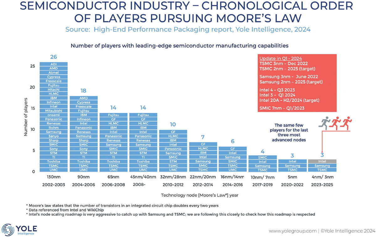
SOURCE: Courtesy of Yole Intelligence: High-End Performance Packaging: 3d/2.5d Integration (2024).
passed Intel (which did not fully adopt the foundry business model until 2021)62 as the most important semiconductor manufacturer and has become the world’s 11th-largest company. As the first to reach the 7 nm technology node in 2016, and then the first to reach the 5 nm node in 2020, TSMC has demonstrated sustained technology leadership over U.S. chip manufacturers. Today, TSMC makes the majority of the newest cutting-edge logic chips globally, having assumed technology leadership over U.S. chip fabricators.63 It is also the world’s highest volume semiconductor manufacturer, which creates advantages for cost and sustainability.
Due to the large capital costs needed to establish a leading-edge fabrication facility today, only three companies in the world—TSMC, Samsung, and Intel—are still able to compete (see Figure 2-3).
___________________
62Intel, 2021, “Intel CEO Pat Gelsinger Announces IDM 2.0 Strategy for Manufacturing, Innovation and Product Leadership,” March 23, https://www.intel.com/content/www/us/en/newsroom/news/idm-manufacturing-innovation-product-leadership.html.
63G. Slater and T. Quillin, 2021, “American Technology Leadership Is Critical to Semiconductor Supply Chain Resiliency,” Intel blog, June 8, https://blogs.intel.com/policy/2021/06/08/american-technology-leadership-is-critical-to-semiconductor-supply-chain-resiliency.
Among these three companies, TSMC leads in making the most advanced chips today, with Samsung and Intel trailing, although threats to this market order exist. Intel has announced its plans to catch up with TSMC. TSMC’s location on the island of Taiwan makes it vulnerable to Chinese interference, while Samsung’s leading-edge South Korean fabs are within artillery range of a hostile North Korea. Furthermore, China is making significant investments in semiconductor technology in a systematic effort to disrupt the sector.
Other key aspects of the semiconductor supply chain also deserve consideration with regard to economic and national security.64 China controls a dominant share of certain required critical minerals,65 and has made major investments in assembly and packaging. Similarly, advanced semiconductor chip test and packaging operations, which enable higher performance, energy efficiency, and density in both leading-edge and some legacy node applications, are provided by firms located almost entirely outside the United States.66 Compound-semiconductor chips are based on non-silicon substrates largely provided today by firms in Japan, South Korea, and the United States,67 although Chinese semiconductor firms are working to gain leadership in this area also.68 These chips are used in power electronics, radio frequency telecommunications, lighting, the electrical grid, electric vehicles, health care devices, and manufacturing technologies today, and have potential to blossom into major new markets.69
___________________
64The U.S. role in semiconductor industry sectors is only briefly summarized here. A detailed breakdown of the U.S. share of various global semiconductor sectors is provided in DOC, 2023, Assessment of the Status of the Microelectronics Industrial Base in the United States. See also M. Griffith and S. Goguichvili, 2021, “The U.S. Needs a Sustained, Comprehensive and Cohesive Semiconductor National Security Effort,” Woodrow Wilson Center, https://www.wilsoncenter.org/blog-post/us-needs-sustained-comprehensive-and-cohesive-semiconductor-national-security-effort, and S. Kahn, A. Mann, and D. Peterson, 2021, “The Semiconductor Supply Chain: Assessing National Competitiveness,” CSET, January, https://cset.georgetown.edu/wp-content/uploads/The-Semiconductor-Supply-Chain-Issue-Brief.pdf.
65J. Choi, 2023, “US Semiconductor Regulations Spawn a ‘Mineral War,’“ Business Korea, September 8, https://www.businesskorea.co.kr/news/articleView.html?idxno=201318; Z. Yang, 2023, “China Just Fought Back in the Semiconductor Export War,” MIT Technology Review, July 10, https://www.technologyreview.com/2023/07/10/1076025/china-export-control-semiconductor-material.
66IBM has a packaging plant in Bromont, Quebec, Canada; Intel’s packaging plants are in Poland and Malaysia. See generally, O. Burkacky, T. Kim, and I. Yeam, 2023, “Advanced Chip Packaging: How Manufacturers Can Play to Win,” McKinsey & Company, May 24, https://www.mckinsey.com/industries/semiconductors/our-insights/advanced-chip-packaging-how-manufacturers-can-play-to-win.
67Markets and Markets, 2023, “Compound Semiconductor Market,” https://www.marketsandmarkets.com/Market-Reports/compound-semiconductor-market-178858112.html.
68Tech Insights, 2023, “Can China Dominate the Power Semiconductor Market?” October 16, https://www.techinsights.com/webinar/can-china-dominate-power-semiconductor-market.
69See, for example, R.F. Service, 2018, “Beyond Silicon: $1.5 Billion U.S. Program to Spur New Types of Computer Chips,” Science, July 24, https://www.science.org/content/article/beyond-silicon-15-billion-us-program-aims-spur-new-types-computer-chips.
This shift in production capacity over the past three decades in large part has been owing to financial support provided by foreign governments,70 which the U.S. government has been unwilling to match until recently. The Semiconductor Industry Association asserts that 70 percent of the higher-total-cost of operations for U.S.-located fabs is driven by industry incentives provided by foreign governments.71
As noted above, U.S. firms do not dominate semiconductor manufacturing as they did through the mid-1980s, but they still are highly competitive in many parts of the semiconductor value chain.72 Although firms in Taiwan and South Korea dominate in advanced logic chip foundry services (TSMC and Samsung), the United States retains strong players in this sector (e.g., Intel, and Abu Dhabi–owned but U.S.-headquartered GlobalFoundries). Likewise, South Korea dominates in memory products (through Samsung and SK Hynix), but U.S.-based Micron remains a strong player in memory products. In chip design, U.S. fabless companies are second to none (these include Nvidia, Apple, Broadcom, AMD, Qualcomm, and many others) and U.S.-based firms Synopsis and Cadence provide world-leading chip design software tools. For semiconductor manufacturing equipment, U.S.-based Applied Materials is a global leader (with about a 20 percent of the global semiconductor equipment market).73
Furthermore, where the United States does not lead, the leading companies are often located in friendly countries. For example, Japanese firms have sustained leadership in some key areas, with a global market share of 56 percent in materials (including vitally important photoresists) and 32 percent in manufacturing equipment.74 Dutch-based Advanced Semiconductor Materials Lithography (ASML)
___________________
70A. Varas, R. Varadarajian, J. Goodrich, and F. Yinug, 2020, “Turning the Tide for Semiconductor Manufacturing in the US,” SIA and Boston Consulting Group, September 6, semiconductors.org/wp-content/uploads/2020/09/Government-Incentives-and-US-Competitiveness-in-Semiconductor-Manufacturing-Sep-2020.pdf, p. 17.
71SIA and Boston Consulting Group, “Strengthening the Global Semiconductor Supply Chain in an Uncertain Era,” Exhibit 16, 34, https://www.semiconductors.org/wp-content/uploads/2021/05/BCG-x-SIA-Strengthening-the-Global-Semiconductor-Value-Chain-April-2021_1.pdf. In Figure 2.3, TCO includes capital expenditure (upfront land, construction, and equipment) plus 10 years of operating expenses (labor, utilities, materials, taxes); “Asian Other” refers to Taiwan and South Korea.
72F. Yinug, 2015, “Made in America: The Facts About Semiconductor Manufacturing, Semiconductor Industry Association,” SIA, August 2, https://www.semiconductors.org/wp-content/uploads/2020/04/SIA-White-Paper-Made-in-America.pdf.
73R. Castellano, 2024, “Applied Materials WFE Market Share Plummets 5% Below ASML in 2023,” Seeking Alpha, March 4, https://seekingalpha.com/article/4675800-applied-materials-wfe-market-share-plummets-5-percent-below-asml-in-2023.
74N. Tochibayashi and N. Kutty, 2023, “How Japan’s Semiconductor Industry Is Leaping into the Future,” World Economic Forum, November 20, https://www.weforum.org/agenda/2023/11/how-japan-s-semiconductor-industry-is-leaping-into-the-future.
effectively has a monopoly on the most advanced lithography systems.75 The CHIPS and Science Act of 2022 (the CHIPS Act) is aimed at strengthening U.S. semiconductor manufacturing, and in sectors of the value chain where the United States is not in a dominant position, there is an opportunity to work to have multiple non-U.S. suppliers in friendly countries.
Additional Challenges: Start-Ups, University Research and Development, and Workforce
Start-ups play a significant role in the U.S. economy generally, but new start-ups in semiconductor fabrication are rare.76 While entry into advanced-node semiconductor production is inevitably limited because of the very large capital requirements, there are new technology areas where innovation may present opportunities for new entrants, such as a possible boom of chip production to fuel an anticipated expansion of AI applications.77 Yet only a small portion of total U.S. venture capital has been invested in U.S. start-ups in semiconductor fields,78 and this has been limited primarily to the seed stage. At the scale-up stage, when start-ups need to bring technologies into production and implementation, foreign capital has been more inclined to invest. For example, among U.S. firms in the semiconductor field seeking to raise Series B- and C-stage capital, a review of 2015 through 2017 shows they had to rely on foreign sources 66 percent of the time.79 U.S. advances, then, are increasingly controlled by foreign investors, and are easily shifted abroad, leading to what some have called the “innovate here, produce there” story.80
In the academic R&D area, while there are strong university departments in semiconductor fields, their ability to conduct research in the most advanced areas is limited by a lack of advanced equipment (an exception is at the SUNY Nanotech campus in Albany, New York).81 Academic departments simply cannot
___________________
75Miller, Chip War, pp. 183–189, 199. See also E. Rasmussen, B. Wilthan, and B. Simonds, 2023, Report from the Extreme Ultraviolet Working Group Meeting: Current State, Needs and Path Forward, NIST, Report No. 1500-208, August 22, https://doi.org/10.6028/NIST.SP.1500-208.
76President’s Council of Advisors on Science and Technology (PCAST), 2022, Report to the President on Revitalizing the Semiconductor Ecosystem, White House, September, https://www.whitehouse.gov/wp-content/uploads/2022/09/PCAST_Semiconductors-Report_Sep2022.pdf.
77K. Hagey and A. Fitch, 2024, “Sam Altman Seeks Trillions of Dollars to Reshape Business of Chips and AI,” Wall Street Journal, February 8, https://www.wsj.com/tech/ai/sam-altman-seeks-trillions-of-dollars-to-reshape-business-of-chips-and-ai-89ab3db0.
78PCAST, 2022, Report to the President on Revitalizing the Semiconductor Ecosystem, pp. 20–23.
79Griffith and Goguichvili, Wilson Center.
80Ibid.
81J.A. del Alamo, D.A. Antoniadis, R.G. Atkins, M.A. Baldo, et al., 2021, “Reasserting U.S. Leadership in Microelectronics—A White Paper on the Role of Universities,” Massachusetts Institute of Technology, https://dspace.mit.edu/handle/1721.1/139740.
afford the extremely expensive equipment, so university research, which is critical for advances in many technology fields, is often unable to keep up with industry advances and to adequately contribute to them. This also affects the numbers of semiconductor scientists and engineers that universities can train. Effective arrangements for shared access to advanced facilities between universities and industry have not been formed, so there is a growing disconnect between industry and academic researchers.82
Workforce is another challenge.83 If the United States is seeking to restore its leadership in semiconductor technology, where is the needed talent going to come from? A recent report from the National Security Commission on Artificial Intelligence articulates the solution succinctly: “Cultivating more potential talent at home and recruiting and retaining more existing talent from foreign countries are the only two options to sustain the U.S. lead.”84 Yet while U.S. college enrollment for computer science majors has soared in recent years, enrollment for engineers with the skills needed to work in semiconductor production fields has declined.85 Salaries in high-paying semiconductor engineering jobs lag behind salaries in software-oriented jobs, where computer scientists and engineers earn more.86 Computer science and engineering programs continue to grow but are software-focused, and semiconductor hardware design and production is generally not included in the curriculum.87 Programs to address this imbalance are required if the United States is to support its leading-edge semiconductor manufacturing capacity.88 Barriers to entry of international talent because of the constraints in the immigration system also affects the available workforce. Equally important is the skilled technical
___________________
82Creating a platform for “chiplet” (an integrated circuit composed of smaller chips where common portions have been designed to support customizable components) design, with supporting software, could focus on designs to demonstrate new innovations and could be one mechanism to improve university as well as start-up design capability. PCAST, 2022, Report to the President on Revitalizing the Semiconductor Ecosystem, p. 22.
83SIA and Oxford Economics, 2023, Chipping Away; NIST, 2023, “R&D Workforce Working Group Update and Recommendations,” NIST Industrial Advisory Committee, February 7, https://www.nist.gov/system/files/documents/2023/02/08/Feb%207%20IAC%20Meeting%20Workforce%20Presentation%20Final.pdf.
84National Security Commission on Artificial Intelligence, 2021, Final Report, https://cybercemetery.unt.edu/nscai/20211005220330/ https://www.nscai.gov, p. 173.
85D. Martin, 2022, “America’s Chip Land Has Another Potential Shortage: Electronics Engineers,” The Register, July 8, https://www.theregister.com/2022/07/08/semiconductor_engineer_shortage.
86J. del Alamo, 2022, “Reasserting U.S. Leadership in Microelectronics,” presentation at MIT, May 6, pp. 12–16. See also MIT White Paper, 2021, “Reasserting U.S. Leadership in Microelectronics—The Role of Universities.”
87B. Nikolic, 2023, “Thoughts on Public–Private Partnerships to Strengthen Semiconductor Design,” Presentation to the committee, August 15.
88See recommendations in PCAST, 2022, Report to the President on Revitalizing the Semiconductor Ecosystem, pp. 16–20.
workforce for semiconductor manufacturing, but there is no comprehensive system in the United States for training and upskilling this workforce.89 These workforce issues are addressed in more detail in Chapter 7.
INTERNATIONAL COMPETITION: THE ROLE OF NATIONAL SUBSIDIES IN SEMICONDUCTOR FABRICATION
Industrial subsidies by foreign nations, summarized below, have reduced the cost of offshore fabs by some 25 to 35 percent compared to those in the United States. Such industrial support was not seriously considered by the United States for the two decades leading up to the 2022 CHIPS Act. Absent this financing support, advanced fab construction progressively shifted out of the United States, creating a critical issue for economic and national security implications.
In recent years, recognizing the importance of chips for its own economic well-being and national security, China has made very significant government investments in semiconductor manufacturing and R&D.90 China’s firms made 35 percent of non-leading-edge chips, known as legacy chips,91 in 2019, and that output has been steadily growing, including through sales to the United States. China has been clear on its strategy, which is to first dominate the market for legacy chips, which are still in widespread use in many industrial sectors, while steadily building up expertise and manufacturing capacity as it works toward hoped-for leadership at the most advanced nodes, thereby moving its semiconductor sector further up the value chain. Chinese chipmakers today are
___________________
89S. Shivakumar, C. Wessner, and T. Howell, 2022, “Reshoring Semiconductor Manufacturing: Addressing the Workforce Challenge,” Center for Strategic and International Studies (CSIS), October 6, https://www.csis.org/analysis/reshoring-semiconductor-manufacturing-addressing-workforce-challenge; J. Gluck, K. Sodhi, and A. Higuchi, 2023, “Community Colleges and the Semiconductor Workforce,” Harvard Belfer Center, June, https://www.belfercenter.org/sites/default/files/files/publication/Community%20Colleges%20and%20the%20Semiconductor%20Workforce_CHIPS%20Series.pdf. See, generally, W.B. Bonvillian and S.E. Sarma, 2021, Workforce Education—A New Roadmap, Cambridge, MA: MIT Press.
90D. Strub, 2019, “China’s Innovation Policy and the Quest for Semiconductor Autonomy—Q&A with Dieter Ernst,” AmCham Shanghai, May 23, https://www.amcham-shanghai.org/en/article/semiconductor-dieter-ernst; D. Ernst, 2016, “China’s Bold Strategy for Semiconductors—Zero Sum Game or Catalyst for Cooperation,” East-West Center Working Paper, Innovation and Economic Growth Series No. 9, September, https://www.eastwestcenter.org/publications/chinas-bold-strategy-semiconductors-zero-sum-game-or-catalyst-cooperation.
91Daxue Consulting, 2022, “China’s Semiconductor Industry Seeking Self-Sufficiency Amid Tensions,” September 28, https://daxueconsulting.com/china-semiconductor-industry; Hunt, 2022, “Sustaining U.S. Competitiveness in Semiconductor Manufacturing,” p. 2; See, generally, SIA, 2022, “China’s Share of Global Chip Sales Now Surpasses Taiwan and Is Closing in on Europe’s and Japan’s,” July 10, https://www.semiconductors.org/chinas-share-of-global-chip-sales-now-surpasses-taiwan-closing-in-on-europe-and-japan.
known to be making every effort to develop 7 nm node logic chips.92 As part of this overall strategy, there are currently concerns that China’s producers will flood the chip market with cut-rate chips (i.e., priced below the actual cost of manufacture) to disrupt the business of current non-Chinese producers, forcing some out of the market, to grow China’s share.
The United States has also become reliant on manufacturing facilities abroad for computer memory chips known as dynamic random-access memory (DRAM) and flash memory. Leading-edge DRAM and flash memory fabrication is dominated by fabs located in South Korea, Japan, and Taiwan,93 although a new U.S. DRAM fab has been announced by Micron.94 While Chinese companies do not today have leading-edge DRAM fabs, they are already approaching near-leading-edge in flash technology. Flash prices have been falling in recent years, driven by cost reductions as well as by stronger competition than for DRAM.95 The dynamics of supply chain resiliency and source diversification for DRAM and flash memory is as much of a concern for the United States as for logic chips.96
Different nations have used different approaches to support and grow their semiconductor industries. Excepting the case of China, the largest form of government support in semiconductor-producing nations has been tax code measures, typically through R&D tax credits, property tax abatements, offsets to corporate taxes, and investment tax credits. To briefly summarize some of the major support elements, semiconductor firms in Taiwan have benefited from government-supported R&D through its Industrial Technology Research Institute (ITRI) collaborative, budgetary support through the tax code, state-owned shares in semiconductor firms, discounted land and infrastructure support, preferential loans,
___________________
92A. Shilov, 2023, “Huawei’s New Mystery 7nm Chip from Chinese Fab Defies US Sanctions,” Tom’s Hardware, August 3, https://www.tomshardware.com/news/huaweis-new-mystery-7nm-chip-from-chinese-fab-defies-us-sanctions; D. Wu and J. Leonard, 2022, “China’s Top Chipmaker Achieves Breakthrough Despite U.S. Curbs,” Bloomberg, July 21, https://www.bloomberg.com/news/articles/2022-07-21/china-s-top-chipmaker-makes-big-tech-advances-despite-us-curbs; Tech Insights, 2022, “7nm SMIC Bitcoin Miner,” July 20, https://www.techinsights.com/blog/disruptive-technology-7nm-smic-minerva-bitcoin-miner; P. Alcorn, 2021, “China’s SMIC Shipping 7nm Chips Reportedly Copied from TSMC,” Tom’s Hardware, July 21, https://www.tomshardware.com/news/china-chipmaker-smics-7nm-process-is-reportedly-copied-from-TSM-tech.
93Hunt, 2022, “Sustaining U.S. Competitiveness in Semiconductor Manufacturing,” CSET, pp. 2, 14–15.
94Micron, 2022, “Micron Announces Historic Investment of Up to $100 Billion to Build a Mega-factory in New York,” October 4, https://investors.micron.com/news-releases/news-release-details/micron-announces-historic-investment-100-billion-build-megafab.
95See, generally, Imarc, “Flash Memory Card Market Report, 2023–2028,” https://www.imarcgroup.com/flash-memory-card-market.
96Hunt, “Sustaining U.S. Competitiveness in Semiconductor Manufacturing,” CSET, pp. 4, 17–18.
workforce training, and hiring credits.97 In South Korea, firms benefit from government R&D support through its Electronic and Telecommunications Research Institute (ETRI), budgetary support through the tax code, low-cost financing, infrastructure support, equipment incentives, and workforce training.98 In China, non-market interventions are much more pervasive. The government has provided semiconductor R&D support and direct funding support of companies through a variety of means, including through state ownership, below-cost financing, below-market equity investment, provision of land at below-market prices, and provision of semiconductor manufacturing equipment.99 While Europe has fallen behind in advanced chip production, it remains home to one of the most important semiconductor R&D facilities, IMEC, headquartered in Belgium, which has become the leading global center for applied industry development and receives a sustained level of governmental support, which today amounts to approximately 18 percent of its annual revenues. Notably, the United States has no comparable institution at this time. Prior to the CHIPS Act, budgetary support through the tax code was the primary government support vehicle. Historically, U.S. government–funded R&D also played a significant role, such as the investments in SEMATECH until 1995. In something of a return to a direct R&D investment strategy, DARPA has recently invested several billion dollars in its Electronics Resurgence Initiative (ERI), which launched in 2015.100
A 2023 study from the Congressional Research Service provides further details on the competitive tools used by other nations in semiconductors; some of its findings regarding Taiwan, South Korea, Japan, Europe, and China are summarized below:101
- Taiwan. Taiwanese firms dominate leading-edge semiconductor production and play a large role in the global semiconductor supply chain, providing chip design, R&D, semiconductor materials, and assembly, packaging, and testing. Exports of semiconductors amount to some 25 percent of
___________________
97OECD, 2019, “Measuring Distortions in International Markets: The Semiconductor Value Chain,” OECD Trade Policy Papers, No. 234, Paris: OECD Publishing, https://read.oecd-ilibrary.org/trade/measuring-distortions-in-international-markets_8fe4491d-en, pp. 17, 60, 47, 54; SIA, 2020, “U.S. Needs Greater Semiconductor Manufacturing Incentives,” Chart on Semiconductor Manufacturing Incentives by Country (300 nm or below), July, https://www.semiconductors.org/wp-content/uploads/2020/07/U.S.-Needs-Greater-Semiconductor-Manufacturing-Incentives-Infographic1.pdf, p. 2.
98OECD, 2019, “Measuring Distortions in International Markets,” pp. 17, 60, 68; SIA, 2020, “U.S. Needs Greater Semiconductor Manufacturing Incentives,” Chart on Semiconductor Manufacturing Incentives by Country (300 nm or below), p. 2.
99OECD, 2019, “Measuring Distortions in International Markets,” pp. 7, 47–54, 68–73, 81, 85–87.
100OECD, 2019, “Measuring Distortions in International Markets,” pp. 31, 60.
101K. Sutter, M. Singh, and J. Sargent, 2023, “Semiconductors and the CHIPS Act: The Global Context,” Congressional Research Service, September 28, https://sgp.fas.org/crs/row/R47558.pdf.
- South Korea. Semiconductors are a critical part of South Korea’s production economy, representing 20 percent of its total exports. South Korea has long provided government support, primarily through ETRI (Electronics and Telecommunications Research Institute), a PPP for domestic semiconductor manufacturing. Included in the South Korean strategy is the passage of laws, like the Special Act to Protect and Foster the National High-Tech Strategic Industry (2022), that afford companies regulatory exemptions and tax incentives to spur R&D and increase production output. In 2023, the tax deduction rate was expanded for critical industries, including semiconductors. This included large firms earning tax credits of up to 15 percent and small to midsize firms earning 16 to 25 percent, with the potential to expand by an additional 10 percent. Additionally, South Korea’s vertically integrated conglomerates, called chaebols, have facilitated scale-up in market segments, such as DRAMs. The South Korean government has a stated goal of increasing its domestic sourcing of semiconductor manufacturing materials, components, and equipment from 30 to 50 percent by the year 2030. South Korea is also investing directly, negotiating with ASML to build a plant in South Korea. U.S. investments are part of the strategy of South Korean companies: South Korea’s Samsung is investing $17 billion in a fabrication plant in Texas and SK Hynix in an $11 billion chip packaging plant.
- Japan. Japan maintains a 9 percent market share of the world’s semiconductor production. The government has deployed investment initiatives like the “Strategy for Semiconductor and Digital Industries” (2021) aimed at sustaining Japan’s current global semiconductor market share and developing new materials beyond silicon, with $6.8 billion in support of domestic semiconductor manufacturing. Japanese firms remain competitive in the production of memory chips, sensors, and power semiconductors. This is evidenced by a 35 percent global market share in semiconductor manufacturing equipment and a 50 percent global market share in the production of semiconductor wafers and photoresists.
Taiwan’s Gross Domestic Product (GDP). The government of Taiwan offers incentives to maintain its semiconductor production, including R&D subsidies, tax and tariff stimulus, science parks, subsidized factory buildings, grants and subsidized credit, and connections with local universities and institutes. Examples of tax incentives in 2023 are tax deductions equal to 25 percent of R&D expenditures and 5 percent of spending on new equipment for firms that domestically innovate in critical technologies sectors, including semiconductors. Other recent government actions have included merging two laboratories into the Taiwan Semiconductor Research Institute and providing support for a new ASML lithography tool manufacturing plant.
- Europe. Led by STMicroelectronics and NXP Semiconductors, European-headquartered firms have 10 percent of the global semiconductor market share and have specialized in particular application markets, including the automotive industry, energy applications, and industrial automation. High-value manufacturing equipment leaders like ASML in lithography (Netherlands) and Aixtron in chemical vapor deposition (Germany) help maintain Europe’s position in advanced and specialized semiconductor manufacturing equipment. Stable government support for four decades has been vital for the success of IMEC (Belgium), the global leader in semiconductor R&D. Following an $11.3 billion investment in 2013, the European Chips Act, approved in 2023, seeks to mobilize nearly $47 billion in public and private investment, with a goal of Europe having a 20 percent share of the global semiconductor market. In response to this initiative, Intel announced it would invest more than $40 billion for a foundry in Germany, an expanded facility in Ireland, an assembly and packaging facility in Italy, and a new assembly and test facility in Poland, as well as build a major R&D center and make longer-term investments. With support from the French government, in 2022, STMicroelectronics and GlobalFoundries announced plans for a $5.7 billion wafer production facility in France. Between 2023 and 2025, the United Kingdom’s government plans to invest up to $245 million, and then more than $1 billion over the following 10 years to support the semiconductor sector in the United Kingdom, with a focus on workforce development to improve the UK industry’s access to semiconductor prototyping and tools, as well as strengthening areas of existing capabilities.
- China. Many of China’s industrial policy approaches toward semiconductors are noted earlier in this chapter. To briefly summarize, those practices include direct industrial production subsidies, grants of land for semiconductor sites, equity support (through government-seeded “guidance funds”) and limited regulatory controls; acquiring technology through foreign company acquisitions and joint ventures; setting goals and targets for expansion of both leading-edge and legacy chip semiconductor production; and loose intellectual property practices. A distinguishing feature of China’s industrial policy is its heavy reliance on below-market subsidies to capital flowing to Chinese semiconductor companies, in contrast to the directly budgeted tax and subsidy expenditures (e.g., R&D, capital, and other subsidies from both home and foreign governments) received by firms headquartered in other industrialized economies.102
___________________
102See Figure 3.2, p. 62 in OECD, 2019, “Measuring Distortions in International Markets.”
The most significant reason semiconductor fabrication, assembly, and testing have shifted out of the United States, historically, is because of the manufacturing cost difference between the United States and other nations. The bulk of the cost difference is not in labor costs, which are not a major component of semiconductor fabrication total costs. Rather, studies suggest that differences in costs are predominantly the result of differences in government subsidies (including tax treatment) for semiconductor fabrication facility investments.103 Prior to the CHIPS Act, U.S. semiconductor producers projected that Asian locations would account for nearly all of expected semiconductor fabrication facility growth.104 These projections made clear that a next generation of fabs was not going to be built in the United States absent a major, sustained policy and investment intervention.
A THIRD GOVERNMENTAL PUBLIC–PRIVATE PARTNERSHIP IN SEMICONDUCTORS: THE CHIPS ACT
Acknowledging these developments and their security and geopolitical implications, in 2020 bipartisan leaders on the U.S. Senate Intelligence Committee introduced major legislation designed to restore U.S. semiconductor technology leadership. The CHIPS Act, which authorized $52 billion for a series of interventions into the semiconductor sector,105 was authorized by Congress in 2020 with strong bipartisan support, with appropriations passed in 2022 to fully fund it. This was structured as a one-time bill, with no assurance of follow-on support for ongoing sector needs when the funding ends after 5 years.
The legislation provided $39 billion of financial assistance for companies to construct or modernize U.S.-located semiconductor fabrication plants and to acquire fabrication equipment (see Appendix D). It also offered a 25 percent investment tax credit for investments in U.S.-located semiconductor manufacturing plants and equipment and a $75 billion loan guarantee program. It further provided $11 billion for semiconductor R&D, including funding to set up an industry–university semiconductor technology center, an advanced packaging R&D program, and new advanced manufacturing institutes for semiconductors. The lead agency for all these efforts was DOC. Funding was also provided for DARPA’s
___________________
103SIA, “U.S. Needs Greater Semiconductor Manufacturing Incentives,” Chart on Semiconductor Manufacturing Incentives by Country (300 nm or below), p. 2; del Alamo, et al., “Reasserting U.S. Leadership in Microelectronics,” pp. 17–18.
104SIA, “U.S. Needs Greater Semiconductor Manufacturing Incentives,” p. 1.
105CHIPS for America Act, S.3933, 116th Cong. 2nd Sess., introduced June 10, 2020, https://www.congress.gov/bill/116th-congress/senate-bill/3933. See also Senator Mark Warner, 2020, “Bipartisan, Bicameral Bill Will Help Bring Production of Semiconductors Back to U.S.,” Press release, June 10, https://www.warner.senate.gov/public/index.cfm/2020/6/bipartisan-bicameral-bill-will-help-bring-production-of-semiconductors-critical-to-national-security-back-to-u-s.
microelectronics R&D initiatives and for a semiconductor workforce education program at NSF. In addition, funding was available for international supply chain collaborations. Overall, interagency coordination is assigned to the White House Office of Science and Technology Policy’s National Science and Technology Council semiconductor subcommittee.
While DOC is the lead agency under the legislation, managing the great bulk of the funding, DoD was not ignored. Prior to the legislation and in many ways anticipating it, DARPA in 2017 began the Electronics Resurgence Initiative (ERI) to develop new semiconductor materials, designs, and architectures;106 this was renewed in 2023 as ERI 2.0 to promote U.S. technology leadership in next-generation microelectronics research, development, and manufacturing,107 and DARPA received additional funding in the CHIPS Act for this program. In addition, DoD’s Office of the Under Secretary of Defense for Research and Engineering received $2 billion in funding over 5 years under the CHIPS Act to create the Microelectronics Commons (ME Commons) program to create a network of industry–university–government PPPs across the country to focus on technology readiness level (TRL) 4–7108 semiconductor sector advances. The initial competitive awards totaling $238 million for eight hubs in DoD focus areas were announced in September 2023.109
Not long after enactment of the CHIPS Act, three major U.S.-based semiconductor companies—Micron, Qualcomm, and GlobalFoundries—announced large commitments to expand their domestic manufacturing facilities to take advantage of the act.110 Intel announced major new semiconductor manufacturing fabs in Ohio and Arizona.111 Samsung (which has also embraced the foundry model)
___________________
106DARPA, 2017, “Beyond Scaling: An Electronics Resurgence Initiative,” June 1, https://www.darpa.mil/news-events/2017-06-01.
107DARPA, 2023, Electronics Resurgence Initiative 2.0, March 6, https://www.darpa.mil/work-with-us/electronics-resurgence-initiative.
108Technology readiness levels (TRLs) are a type of measurement system used to assess the maturity level of a particular technology. Each technology project is evaluated against the parameters for each technology level and is then assigned a TRL rating based on the projects progress. There are nine technology readiness levels. TRL 1 is the lowest and TRL 9 is the highest. https://www.nasa.gov/directorates/somd/space-communications-navigation-program/technology-readiness-levels.
109DoD, 2023, “Deputy Secretary of Defense Kathleen Hicks Announces $238M CHIPS and Science Act Award,” September 20, https://www.defense.gov/News/Releases/Release/Article/3531768/deputy-secretary-of-defense-kathleen-hicks-announces-238m-chips-and-science-act.
110Micron, 2022, “Micron Announces $40 Billion Investment in Leading-Edge Memory Manufacturing in the US,” August 9, https://investors.micron.com/news-releases/news-release-details/micron-announces-40-billion-investment-leading-edge-memory; GlobalFoundries. 2022, “GlobalFoundries and Qualcomm Announce Extension of Long-Term Agreement to Secure U.S. Supply Through 2028,” August 8, https://gf.com/gf-press-release/globalfoundries-and-qualcomm-announce-extension-of-long-term-agreement-to-secure-u-s-supply-through-2028.
111Intel, 2022, “Implementing a Great Step Forward in Competition Policy,” August 8, https://community.intel.com/t5/Blogs/Intel/Policy-Intel/Implementing-a-Great-Step-Forward-in-Competition-Policy/post/1406902.
has an existing fab in Austin, Texas, and is planning to open a new one nearby in 2024.112 TSMC has announced three new fabs in Phoenix, Arizona (its first in the United States), to produce at the 5 and 3 nm scale, although opening has been delayed somewhat owing to workforce recruiting issues.113
The CHIPS Act provided a strong signal of U.S unity on the policy goal of retaining a robust semiconductor manufacturing industry deploying state-of-the-art (SOTA) technology. However, with the cost of a single advanced volume-scale fab approaching $20 billion, and roughly equivalent levels of resources required to develop the next generation of fabrication process technology, the level of funding and 5-year commitment in the CHIPS Act will not be sufficient for maintaining an edge capability. Some observers have argued that U.S. manufacturing industry in general has faced hollowing out from decades of disconnect between production and R&D systems; financial sector focus on core competency, which reduced supply chain resiliency; financialization; production offshoring; and underinvestment in advanced production.114 A number of these problems have seeped into semiconductor production, and it is not clear whether the CHIPS Act will be adequate to reverse these trends. It may stem the decline in chip production facilities in the United States and boost U.S. global production share only modestly. Nonetheless, the act marked a major government intervention into the sector at an unprecedented funding level, even though a longer-term continuing commitment will likely be required to meet the stated objectives.
ACCOMPANYING EXPORT CONTROLS
On October 7, 2022, DOC announced significant export controls on China’s semiconductor sector, applying restrictions particularly to exports of tools and equipment used to manufacture semiconductors.115 The move marked a change in U.S. policy which, starting with China’s entry into the World Trade Organization in 2001, had sought to integrate China’s economy into a global system on the
___________________
112S. Kim and I. King, 2022, “Samsung Woos US Chip Buyers with Tech Advances, Texas Focus,” Bloomberg, October 3, https://www.bloomberg.com/news/articles/2022-10-03/samsung-woos-us-chip-buyers-with-tech-advances-texas-production.
113H. Charlton, 2021, “Apple’s Chip Partner TSMC to Begin Mass Production of 5nm Chips at New Arizona Factory in 2024,” MacRumors, July 15, https://www.macrumors.com/2021/07/15/tsmc-arizona-factory-begin-production-in-2024; K. Stone, 2023, “TSMC Delays Start of Phoenix Chip Factory, Citing Skilled Worker Shortage,” KTAR News, July 21, https://ktar.com/story/5519118/tsmc-delays-start-of-phoenix-chip-factory-production-until-2025-because-of-skilled-worker-shortage.
114D. Adler and W.B. Bonvillian, 2023, “America’s Advanced Manufacturing Problem and How to Fix It,” American Affairs 7(3), https://americanaffairsjournal.org/2023/08/americas-advanced-manufacturing-problem-and-how-to-fix-it.
115J. Schneider and I. Zhang, 2022, “New Chip Export Controls and the Sullivan Tech Doctrine,” ChinaTalk, October 11, https://www.chinatalk.media/p/new-chip-export-controls-explained.
assumption that a freer Chinese economy would lead to a freer political system and increased adherence to international market laws and norms. With China’s increasingly authoritarian rule, expanding military power, and threats to Taiwan, that assumption is increasingly called into question. Following the announcement of the new export controls, stock valuation declined in semiconductor firms both in China (since limiting access to advanced chip production equipment may affect their ability to expand) and the United States (because of concerns that access to Chinese markets that many U.S. firms depend on will be limited).116 Questions have arisen concerning the initial effectiveness of these controls,117 and some U.S. semiconductor firms are objecting to further controls because of their dependence on maintaining market share in China.118 China accounts for approximately one-third of the global semiconductor market and more than $50 billion in combined annual revenue for Nvidia, Intel, and Qualcomm.
The new U.S. export controls are seen by many as part of a global technology “decoupling” that began 7 years ago with China’s “Made in China 2025” plan to achieve technology leadership in key technology sectors and make its own economy more self-sufficient.119 Past history suggests the effectiveness of export controls inevitably fades over time, and the only sustainable way to stay ahead in a technology competition is to retain technology development leadership. This includes maintaining significant R&D with dynamic industry participation, working to bring innovations to market first, and maintaining competitive differentiation. Technology leadership likely needs to be the central thrust of the U.S. and DoD policy approaches, while recognizing that the semiconductor industry is now truly a global one. While the United States may be able to slow the rate of advances in China for a time, leading-edge semiconductor fabrication is unlikely to return to the state of asymmetric U.S. dominance observed at the start of the 21st century, regardless of the CHIPS Act incentives and export controls. Collaboration in
___________________
116I. Morris, 2023, “US Chip Exposure to China Grew Even More Last Year,” Chart (from SEC data on U.S. chipmaker companies’ sales to China, 2017–2022), Light Reading, March 24, https://www.lightreading.com/semiconductorsnetwork-platforms/us-chip-exposure-to-china-grew-even-more-last-year/d/d-id/784025.
117T. Fist, L. Helm, and J. Schneider, 2023, “Chinese Firms Are Evading Chip Export Controls,” Foreign Policy, June 21, https://foreignpolicy.com/2023/06/21/china-united-states-semiconductor-chips-sanctions-evasion; D. Patel, A. Ahmad, and M. Xie, 2023, “China AI & Semiconductors Rise: U.S. Sanctions Have Failed,” Semianalysis, September 12, https://www.semianalysis.com/p/china-ai-and-semiconductors-rise.
118T. Mickle, D. McCabe, and A. Swanson, 2023, “How the Big Chip Makers Are Pushing Back on Biden’s China Agenda,” New York Times, October 5, https://www.nytimes.com/2023/10/05/technology/chip-makers-china-lobbying.html.
119R. Fordoohar, 2022, “We Must Prepare for the Reality of the Chip Wars,” Financial Times, October 27, https://www.ft.com/content/ef90d296-627d-4ff9-9983-ff537bdb078b.
technology development with friendly nations will continue to be valuable for the semiconductor sector, as it is in addressing climate change and other global challenges.
NATIONAL SECURITY AND ECONOMIC SECURITY ISSUES
During the later stages of the Cold War, the U.S. government and DoD, led by Defense Secretary Harold Brown and Under Secretary William Perry, articulated what it called an “offset” strategy whereby the United States would offset Soviet advantages in numbers with superiority in technology.120 In many respects, this was a renewal of a strategy that dated back to the accelerated, early adoption of cutting-edge technology by the U.S. military in the 1950s and 1960s, as previously discussed. Computer chips were crucial to that strategy, enabling the United States to develop precision weapons that led to a decisive military superiority. Russia effectively missed the information technology (IT) revolution, so was not able to compete with these developing military systems. DoD has found that China’s growing technology prowess makes it a greater national security challenge.121 China’s application of an industrial policy approach with very significant subsidies, which the United States has not in the past attempted to match,122 has allowed China to capture key emerging technology sectors, with semiconductor leadership now a top Chinese priority. China is also turning both more insular and more assertive, with the state reassuming strong control of the technological agenda, moving it away from software-based social media firms toward growing government support and funding for hardware technologies.
Although DoD dominated semiconductor markets in the first two decades of the industry’s history, it now accounts for only a tiny share, less than 2 percent, of the total. Furthermore, the bulk of DoD’s needs today are for legacy chips: only 11 percent of its spending is for chips with critical dimensions under 28 nm, 18 percent is for chips between 28 and 90 nm, and 66 percent for chips between
___________________
120Office of the Secretary of Defense, 2018, “Harold Brown: Offsetting the Soviet Military Challenge, 1977–1981,” Historical Office, March 5, https://history.defense.gov/Portals/70/Documents/speaker_series/webHaroldBrownProgram2018.pdf.
121DoD, 2022, “Military and Security Developments Involving the People’s Republic of China,” Annual Report to Congress, https://media.defense.gov/2022/Nov/29/2003122279/-1/-1/1/2022-Military-and-Security-Developments-Involving-The-Peoples-Republic-of-China.pdf.
122G. DiPippo, I. Mazzocco, S. Kenedy, and M. Goodman, 2022, “Red Ink: Estimating Chinese Industrial Policy Spending in Comparative Perspective,” Center for Strategic and International Studies (CSIS), May 23, https://www.csis.org/analysis/red-ink-estimating-chinese-industrial-policy-spending-comparative-perspective; D. Adler, 2022, “Guiding Finance: China’s Strategy for Funding Advanced Technologies,” American Affairs 6(2), https://americanaffairsjournal.org/2022/05/guiding-finance-chinas-strategy-for-funding-advanced-manufacturing. Regarding semiconductors, see OECD, 2019, “Measuring Distortions in International Markets,” pp. 55–85.
90 and 350 nm.123 DoD utilizes chips in its systems that are typically two generations or more from the cutting-edge. Its custom-designed application-specific integrated circuit (ASIC) chips are fabricated in approved “trusted foundries” in the United States, for security reasons, on manufacturing lines that often lag even further from the leading-edge. These facilities will continue to be important for DoD, especially as innovation at legacy nodes continues—for example, in automotive applications.
However, new defense-related technologies are very likely to push DoD toward increasing reliance on more advanced chips. The military will require use of the most advanced available artificial intelligence (AI) coprocessor chips as AI capabilities are deployed for applications ranging from automating development of software and firmware to being inserted into military systems as a critical new tool of warfare. DoD will also require leading-edge chips for its advanced data fusion centers, autonomous platform technologies, advanced sensor systems, distributed cloud computing, and promising defense applications emerging from quantum IT. These advances will require DoD to field new software and systems, running on chips with the lowest possible power consumption, lowest possible weight, and greatest possible density, to respond to potential adversaries. In addition, because weapons platforms like aircraft and ships must last for decades, over time these must be modernized to incorporate new capabilities, and DoD needs advanced chips for these modernization initiatives. Chiplets and other more advanced electronics capabilities are expected to emerge more rapidly in the future; therefore, software and hardware updates need to be accommodated effectively and efficiently on a much more frequent basis, as well as factored into the design process for new equipment.
Other advances are on the horizon. On-chip silicon structures have been evolving from a two-dimensional (2D) approach to a focus on three-dimensional (3D) architectures. The heterogeneous integration of “chiplets” into 3D packages containing multiple chips, perhaps each produced using different processing technologies and materials, is evolving rapidly.124 New computer architectures that overcome energy efficiency limits and eliminate barriers to rapid access to data in memory, photonic interconnects, electronic design automation to make custom
___________________
123DOC, 2023, Assessment of the Status of the Microelectronics Industrial Base in the United States, Table, Respondent End Use Projections—Percent of Chips Segment Revenue, U.S. Defense; Table, Respondent End Use Projections—Percent of End Use Revenue for Given Nodes, U.S. Defense. See also D.J. Radack, B.S. Cohen, R.F. Leheny, V. Sharma, and M.M.G. Slusarczuk, 2016, Semiconductor Industrial Base Focus Study—Final Report, Institute for Defense Analyses.
124See, for example, S. Zhang, Z. Li, H. Zhou, S. Wong, R. Li, S. Wang, K. Paik, and P. He, 2022, “Challenges and Recent Prospectives of 3D Heterogeneous Integration,” e-Prime—Advances in Electrical Engineering, Electronics and Energy 2, https://www.sciencedirect.com/science/article/pii/S2772671122000249.
circuit design less expensive, and specialized architectures that optimize computing performance for specific applications are being actively explored.125 As current transistor device technologies hit scaling limits over the next decade, new post-complementary metal-oxide-semiconductor (post-CMOS) transistor technologies are emerging.
Inevitably, DoD will increasingly be functioning as a high-end customer in the advanced chip market. DoD grasps this reality; the security of the industrial base on which it depends is increasingly a key focus for national security.126 That is, today DoD understands that the lack of a healthy advanced semiconductor manufacturing sector in the United States will compromise its defense capability.
It is clear to the committee that the United States will not be able to replicate a standalone national supply chain—entrenched specialization and comparative advantage across the supply chain and steep capital and R&D costs preclude this. Given that semiconductor independence is not economically feasible, DoD needs to determine which strategic semiconductor partnerships it requires to assure a diversified and reasonably secure supply chain, with both redundancy and competitive access. The United States has many strengths, including its R&D base, the remaining U.S. firms, the depth of its market, and its ability to create global alliances guaranteeing security in semiconductor manufacturing capability.
The committee is confident that the United States can retain a significant and robust position in leading-edge, commercial semiconductor manufacturing with new strategies and support mechanisms. Key to success will be ensuring some protection for critical domestic links in supply chains and nurturing key U.S. production elements—that is, “onshoring.” However, a secure ecosystem will also require a network of multiple suppliers located in both the United States and in friendly nations to meet DoD objectives, which means maintaining a complex web of multinational relationships—”friend-shoring.”127
The CHIPS Act has a 5-year focus, whereas the issues described above are longer-term challenges that DoD faces. Therefore, there are two ongoing transitions: a transition to new DoD system designs that incorporate the most advanced semiconductors available, which is paralleled by preparation for more
___________________
125OSTP, 2022, “Draft National Strategy for Microelectronics Research,” pp. 8–9.
126DoD, 2022, National Defense Strategy, October 27, https://www.defense.gov/National-Defense-Strategy; OSTP, 2022, “Draft National Strategy for Microelectronics Research, Comments of the SIA on OSTP Request for Information,” October 17, https://www.semiconductors.org/wp-content/uploads/2022/10/OSTP-National-Micro-Strategy-RFI-Response-SIA-FINAL.pdf, pp. 1–2.
127OSTP, 2022, “Draft National Strategy for Microelectronics Research,” pp. 1–2, 4. See also SIA and Boston Consulting Group, 2021, “Strengthening the Global Semiconductor Supply Chain in an Uncertain Era,” SIA, April, https://www.semiconductors.org/wp-content/uploads/2021/05/BCG-x-SIA-Strengthening-the-Global-Semiconductor-Value-Chain-April-2021_1.pdf, pp. 27–38.
disruptive technologies on the horizon. DoD has in recent decades often chosen to prioritize access to secure chips over access to advanced chips; its need for upcoming disruptive technology advances enabled by advanced semiconductors will require it to rethink this balance, as discussed in Chapter 5. DoD will also need strategic international partnerships to achieve these objectives throughout the coming decade.
LESSONS FOR THE DEPARTMENT OF DEFENSE FROM SEMICONDUCTOR HISTORY
Technological and economic drivers have been central to the evolution of the global semiconductor industry over the last five decades, and understanding how they have changed is critical to a successful DoD semiconductor strategy.
Leading-Edge Chip Costs Are Declining More Slowly Compared with Previous Trends
The primary technological reality from about the early 1960s through the first decade of the 21st century was that the area occupied by an electronic device on a silicon chip (transistor density), the speed of the device (transistor switching time), power used per electronic device (energy used per transistor), and manufacturing cost per device (transistor cost) all improved rapidly, in concert, owing to what came to be known as Dennard scaling.128 However, the steady flow of technological improvements for creating 2D structures on the surface of a silicon wafer has slowed considerably over the past decade, as leading-edge fabrication technology shifted toward more complex 3D electronic device structures. The net result is that while device size, speed, and density continue to improve with new generations of silicon fabrication technology, cost declines have lessened compared with previous historical trends. Figure 2-4 reflects one large semiconductor company’s view of electronic device performance and costs at recent technology nodes.129
___________________
128The underlying theory of Dennard scaling suggested that a 30 percent reduction in transistor feature size, associated with a 50 percent reduction in transistor area, would be accompanied by a 30 percent reduction in delay (40 percent increase in clock frequency) and a 50 percent reduction in power. See H.E. Esmaeilzadeh et al., 2013, “Power Challenges May End the Multicore Era,” Communications of the ACM 56(2):95.
129For additional discussion on the flattening out of cost declines at recent nodes, including data for both fabless and foundry semiconductor companies, see K. Flamm, 2018, “Measuring Moore’s Law: Evidence from Price, Cost, and Quality Indexes,” Working Paper 24553, National Bureau of Economic Research, https://doi.org/10.3386/w24553, April; C. Corrado, J. Haskel, J. Miranda, and D. Sichel, eds., 2021, Measuring and Accounting for Innovation in the Twenty-First Century, Chicago: University of Chicago Press and National Bureau of Economic Research, pp. 417–419.
SOURCE: Adapted from Marvell Technology, Inc., Investor Day 2020 Presentation, https://filecache.investorroom.com/mr5ir_marvell/131/download/Marvell%20Investor%20Day%202020.pdf. Reprinted with permission from Marvell, © 2020.
For DoD to achieve its goal of uncontested technological superiority over potential adversaries—which has been the central organizing tenet underlying post–World War II national security strategy—it continues to seek weapons systems that achieve the highest possible performance with the lowest possible power requirements and with the highest possible density (smallest size and lightest weight). With the electronics that power this technological advantage no longer falling in cost at historic rates, or perhaps even increasing in cost, DoD should be prepared to once again invest substantial sums in achieving the technological superiority needed to offset numerically superior adversaries, as it did in the 1950s and 1960s.
Economies of Scale
Increasing economies of scale (i.e., the average cost per unit declines with increased output of units) in chip fabrication now make leading-edge chip designs relatively more expensive in low volumes than in the past, primarily because of fixed production costs that do not vary with production volume. That is, costs per chip are now often dominated by very large, fixed costs. The principal fixed cost drivers for increasing economies of scale in chip fabrication are as follows: the ever-greater investments needed to build a leading-edge fab, the escalating costs of creating mask sets
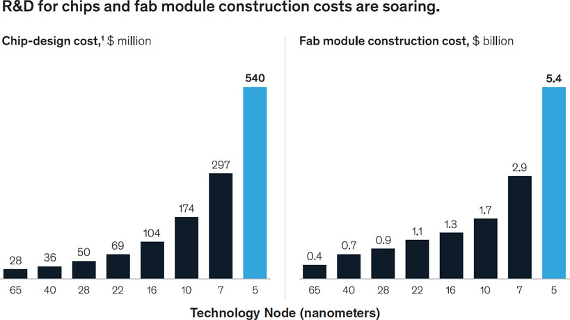
NOTES: Footnote 1 defined as major components include intellectual property qualification, architecture, verification, physical, software, prototyping, and validation. R&D, research and development.
SOURCE: Courtesy of McKinsey & Company: Industrials and Electronics.
(reticles), the larger numbers of masks and processing steps required; and the soaring fixed costs of designing, verifying, prototyping, and validating new chip designs. (See Figure 2-5 for design costs per chip and investment costs per wafer fab module.)
The net effect of rapidly increasing fixed investment costs for the newest technology nodes has been to create economic advantage for the largest volume manufacturers, which in turn has led to industry consolidation over time. Today, the per-wafer costs of manufacturing semiconductors are much higher at low volumes of output than historically has been the case (see Figure 2-6). While there are many more transistors per wafer at the most advanced technology node, Figure 2-4 illustrates that cost per leading-edge transistor for even large fabless semiconductor producers like Marvell has risen at the typical volumes at which their most advanced chip designs are manufactured and sold.
Indeed, there has been increasing concentration in virtually every segment of the semiconductor industry (including semiconductor equipment and materials) in the 20th and early 21st century, driven by economies of scale. In the 20th century postwar period, many computer manufacturers had their own captive fabs churning out custom chips for use in their computer products. Increasing economies of scale led those computer companies to outsource their chip designs to foundries and drop out of chip manufacturing one by one—with the last to leave
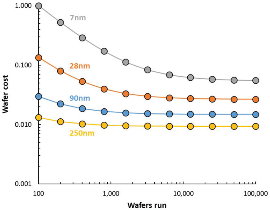
SOURCE: Courtesy of Dylan Patel of SemiAnalysis.
being IBM, in the 21st century. Many companies followed the same path, shifting to so-called “fab-lite” models or even “fabless” business models. Most of today’s U.S. semiconductor industry sales are composed of semiconductors designed in the United States but manufactured at facilities scattered around the globe, using inputs sourced from a thoroughly globalized materials and equipment industry. These developments create growing cost containment problems for DoD, which is often in the position of being a low-volume customer seeking customized chips.
Investments in Research and Development
Historically, U.S. technology leadership has led to better outcomes than efforts to control the global diffusion of technology through export controls, which are costly in terms of political and economic capital and rarely work over the long term. There are notable examples of this pattern within the semiconductor sector. Development of germanium transistors in the United States was quickly copied abroad in the 1950s. Rather than impeding imports, the U.S. semiconductor
industry invested in development of silicon transistors, which ultimately displaced the lower-performance germanium devices. When foreign producers became competitive in silicon transistors, U.S. chip producers moved on to integrated circuits. When foreign producers successfully copied—and improved on—U.S. memory integrated circuits, U.S. producers moved on to new kinds of circuits, including microprocessors and digital signal processors. When foreign computer manufacturers succeeded in producing competitive mainframes and supercomputers, U.S. producers developed new machines using novel parallel architectures, high-performance processor interconnection fabrics, and other architectural innovations, like reduced instruction set computers (RISC).
As noted, a major transition to post-CMOS technologies is now in view. Experience shows that export controls can create a measure of success in slowing down and making more costly the technological development of a rival or potential adversary in the short- to medium-run. But historically, export controls have not prevented the diffusion of technology in the long-run. However, strategic advantage can only be maintained by investing in the next generation of technology. This suggests that DoD’s interests will be best served not by relying simply on export controls but also by striving for technology leadership, which creates both strategic advantage for DoD (when inserted into DoD systems) and competitive advantage for the U.S. firms pioneering new products serving both commercial and defense applications.
It is important to recognize that R&D in both next-generation (i.e., post-CMOS, as discussed further in Chapter 3) semiconductors and in design innovation will be important to DoD’s continued success. The CHIPS Act focused on manufacturing facilities, but with chip design costs soaring at recent technology nodes, reducing the cost of chip designs for specialized DoD needs is another critical problem for DoD. DoD is not alone; this problem is shared by start-ups and small to midsized firms trying to establish markets for innovative system designs that require advanced chips. This is a key area where strong alignment and better program integration between DoD and DOC can yield substantial economic and security benefits for the nation.


